The MATQu project follows a standard work package structure consisting of five technical work packages (WP1 – WP5) enclosed by two non-technical work packages (WP6 and WP7)
- WP 1 – Specific High Resistivity & Low defectivity substrates
- WP 2 – Materials, modules & processes for superconducting qbits
- WP 3 – 3D packaging & bonding
- WP 4 – Characterization tools & Benchmarking
- WP 5 – Simulation & Characterization Demonstrators
- WP 6 – Dissemination & Communication
- WP 7 – Management
RF-SOI substrates are thought to be a good enabler to fabricate high performance superconducting qubit devices. In this intermediate report, relevant substrates parameters have been identified in order to maximize the performance of superconducting resonators, by limiting microwave losses. A new resonator process flow for 300mm SOI wafers has been developed, with a new dedicated mask set, including various structures designed by several partners, in order to investigate the losses over several orders of magnitude.
In this intermediate report on the achieved status for the high resistive 300mm Si substrate wafers we summarized the agreed specification for the substrates, the developed crystal growth process, characterization data for the grown crystal and the wafer data for the first Si wafer sample which was send to the Partner IMEC for resonator tests and Q-factor evaluations.
The deliverable presents the fabrication of superconducting resonators using CMOS compatible platforms, on bulk substrates (IMEC) and SOI substrates (CEA), and the first results on their characterization.
Standardized methodology for superconducting resonator testing was proposed across the consortium to enable unambiguous intercomparability across the different testing laboratories. Test resonator designs were created to support the activities by several partners aiming to find improved materials and fabrication processes for quantum computing applications.
Three different tailor-made high-performance photoresist-stripper formulations were developed within the MATQu project. All formulations are water-based and revealed no etching towards critical TiN layers. Comprehensive studies were carried out. Therefore, time dependent measurements and different types of plasma-etch pretreaments were investigated.
In this Deliverable, Fraunhofer IPMS has screened different superconducting materials, paying special attention to deposition of CMOS-compatible superconducting materials such as silicides, TiN or TaN. A final optimized flow for the integration of Superconducting resonators using TiN as reference material has been developed.
A transmon qubit is formed by shunting a Josephson junction with an extremely low-loss capacitor. In the vast majority of presently fabricated superconducting qubits, with coherence times comparable to state of the art, the Josephson junctions are superconductor-insulator-superconductor (SIS) junctions formed by shadow angle evaporation and lift-off of aluminum, typically on small coupons. In this report, we describe our progress in moving this conventional process onto full-wafer tools and in developing alternative junction fabrication process which does not use lift-off. Abandoning lift-off has the potential to improve yield, parameter control, and process compatibility with other processing steps. Here, we have, especially, investigated and utilized the side-wall spacer passivated (SWAPS) tunnel junction fabrication technique.
A transmon qubit is formed by shunting a Josephson junction with an extremely low-loss capacitor. In the vast majority of presently fabricated superconducting qubits, with coherence times comparable to state of the art, the Josephson junctions are superconductor-insulator-superconductor (SIS) junctions formed by shadow angle evaporation and lift-off of aluminum, typically on small coupons. In this report, we describe our progress in moving this conventional process onto full-wafer tools and in developing alternative junction fabrication process which does not use lift-off. Abandoning lift-off has the potential to improve yield, parameter control, and process compatibility with other processing steps. Here, we have, especially, investigated and utilized the side-wall spacer passivated (SWAPS) tunnel junction fabrication technique.
In this report IQM, VTT and IMEC have assessed the performances of different resonators taking into account variability. This is an important aspect in the long-term perspective of large-scale qubit integration since a tight control over resonator characteristics is needed. Besides that, assessing variability at cryogenic temperatures is a formidable task as the measurement throughput is very low compared to devices operated at room temperature. This task has been tackled evaluating the spread of resonator Q factors within a chip and across different wafers for different materials, geometries of the resonators and chips packaging. We have also obtained the distribution of the resonance frequencies of the different resonators that can ultimately serve as feedback to design and integration.
Indium deposition on copper and on superconductive substrates on wafer scale ongoing at imec.
A novel formulation for photoresist stripping and fluoropolymer removal has been successfully developed. The formulation features low substrate cleaning times. The internal quality and upscaling qualification process has been passed and, therefore, the mixture is ready to be produced and shipped in industrial scale for machine testings.
In this report direct electrodeposition of indium on SC layers using an optimized electrolyte from Atotech is introduced. Using the plated wafers, indium to indium bump and indium to SC layers bonding is performed. An atmospheric plasma cleaning process to clean the indium native oxide using reducing gas followed by bump passivation prior to thermocompression bonding (TCB) process is developed. TCB process is performed at air. Plasma-treated indium surface is characterized by contact angle, Fourier-transform infrared spectroscopy, and X-ray Photoelectron Spectroscopy methods. A successful bonding process of In-In and In-SC layers using a test vehicle with 20, 10, 7, and 5 um pitch bumps is achieved when samples are cleaned by plasma. Mechanical stability of bonded samples was characterized by cross section SEM and die shear. These results show high applicability of plasma-treated indium bumps with successful flip chip bonding at low temperatures and air atmosphere. Furthermore, IMC growth is studied between SC layers and indium using an in-situ resistance measurement at different temperatures and different times. The results show no IMC growth between Nb-In and TiN-In layers. At temperatures close to melting point of indium a sharp increase can be seen in the resistance value.
New 3D-integration routes for superconducting Josephson junction qubits include the development of an interposer die with through‑silicon vias (TSV) for vertical and compact interconnections. Since fluoropolymer dielectric residues remaining in the vias may be detrimental for subsequent processes or qubit functionality, they must be removed without damaging the structure or other materials. Therefore, we developed a new O2 plasma free, selective and non-toxic wet cleaning solution that can remove both the fluoropolymer from the vias and the photoresist used for TSV patterning from the surface. SEM and time-of-flight secondary ion mass spectrometry (ToF-SIMS) analyses confirm complete removal of fluoropolymer residue from the vias. These encouraging results confirm a viable, manufacturable one-step wet cleaning process for TSVs designed for 3D packaging of qubits and other applications.
Besi has developed thermo-compression bonding (TCB) tool called TCnext which allows for in-situ plasma activation of the material to remove oxide layers from the Indium bumps followed by die-to-wafer bonding at low temperature in an inert-gas environment. This tool is commercial tool with dual bond head for high throughput, accuracy around 1µm in X and Y directions and tilt less than 1µm which is necessary for quantum chips stacking with capacitive interconnects.
This report presents the cabling specifications discussed with project partners and summarizes results of prototypes.
Orange QS has designed a comprehensive Quantify-based qubit diagnostics framework for testing multi-qubit quantum chips. The framework is organized in different complexity classes up to the level of qubit gate fidelities, crosstalk characterization and quantum chip benchmarking with a VQE algorithm. The results are summarized in a report.
Kiutra has identified characterization tasks that could significantly benefit from a rapid test system for cryogenic temperatures and derived the adaptations to the cryostat prototype needed for their implementation. The results of our analysis were summarized in a report.
This report states the plan on the dissemination and communication activities of the project.
This report states an update on the dissemination and communication activities of the project.
The project Kick-off meeting took place on June 17th, 2021.
The first half-term report describes the work carried out in the MATQu project from project months one to six.
The second half-term report describes the work carried out in the MATQu project from project months 13 to 18.
Standardized methodology for superconducting resonator testing was proposed across the consortium to enable unambiguous intercomparability across the different testing laboratories. Test resonator designs were created to support the activities by several partners aiming to find improved materials and fabrication processes for quantum computing applications.
IFC successfully developed a prototype product for the fast removal of a pCAR photoresist from a Si-wafer. The prototype reveals a high compatibility towards TiN, proven by etch rate determination methods and surface roughening analyses.
See corresponding Deliverable D2.4
See corresponding Deliverable D2.5
IMEC has worked on the different process modules leading to qubit integration. Leveraging its 300mm integration platform Resonators and Josephson junctions were successfully integrated in a fully substractive etch process.
The consortium-level goals for resonator quality factor and coherence time metrics were consolidated and general instructions on data quality and statistics were created.
The Spherolyte In process was successfully adjusted and applied to deposit indium bumps on substrates with thin copper seed layers. Spherolyte In SC was successfully developed and applied to deposit indium on substrates with superconductive seed layers (e.g. Mo).
Optimization ongoing in collaboration with imec.
Technic Through Silicon Vias (TSV) cleaning blends, photoresist strippers, as well as wet etchant solutions (TiN, Nb, Cu) have been evaluated on wafers provided by partners (IMEC and CEA). Reduction of scallop effect in TSV has also been investigated.
Compatibility of the deposited indium with the CMP process could be shown in collaboration with imec.
Elevate Indium D4900 solution has been validated for indium deposition (thin film and bumps) over copper and ruthenium seed layers. New products have been developed for TSV cleaning: TechniClean D-BOS series. TechniStrip® solutions dedicated to photoresist stripping have been determined to be compatible with Indium and superconductor materials (Nb, NbN, TaN). A new wet etching solution is under development to etch Niobium selectively to Indium.
Indium plated wafers (blanket and patterned) have been provided to partners for further characterization analyses (critical temperature, intermetallic cross-section observation, and reflow tests). A new wet etching solution is under development to etch Ruthenium selectively to Indium, that will enable the optimization of the full process of deposition and etching.
Intelligent fluids has developed a highly performant water-based formulation for TSV cleaning. The novel formulation has passed the internal qualification process. First technical scale production of the prototype was produced for delivery of the material to the collaboration partner IMEC.
Technic provided all desired information (MSDS, TDS) to partners (imec, CEA) for the Elevate Indium D4900 before an upcoming supply. Technic is also ready to supply TechniClean D-BOS for TSV cleaning and TechniStrip® various solutions for photoresist stripping, such as P1331 and MLO07. Innovative selective wet etching solutions for Nb and Ru, while being compatible with In bumps were validated on patterned small size vehicles but necessitate complementary work with partners for industrial validation on full wafer.
Flying wafers with one superconducting routing level and under bump metallization have been provided to partners (Technic and BESI) for In plating and stacking studies. The bottom wafers with In and the top dies are available to make daisy chains.
See corresponding Deliverable D3.5
Chemical mechanical polishing (CMP) of indium is investigated, with the goal of obtaining high quality indium via bond pads for later cryo-3D integration of quantum computing chips, through bonding between these via pads and indium bumps. Higher removal rates were obtained with soft CMP polishing pads than with hard pads. The latter led to deep scratching, while this effect was much more limited for soft pads. For soft pad CMP on patterned wafers, indium is cleared from the Si field in structured areas, leading to relatively high-quality indium surfaces inside bond pads, suitable for 3D die-to-die and wafer-to-wafer bonding.
IFC has developed and optimized a tailor-made intelligent fluid (IF) formulation fur substrate/surface cleaning processes. Optimized process conditions were evaluated and optimized. The novel fluid formulation has been produced in large scale (i.e., 5 L/10 L/20 L canisters, 200 L drum, and 1000 L IBC) to be provided to project partners in high volume.
Alpha phase Ta deposition is developed at room temperature to act as SC layer for TSV connections at cryogenic temperatures. XRD, Rs, AFM and reflectivity measurement show alpha phase Ta deposition when deposited on seed layer of TaN. Without TaN beta phase Ta which has very high resistivity is obtained. Conformality of α-Ta deposition inside the TSV is investigated with FIB and proved good deposition on top, middle and bottom of TSVs.
Kiutra has completed the assembly of the basic ADR cryostat prototype and reported on its performance.
In order to demonstrate the shielding performance of the cryostat prototype a set of high-frequency measurements of typical, highly field-sensitive superconducting resonators have been conducted. The measurements show that the prototype equipped with the magnetic shielding can perform high-quality measurements on all typical types of superconducting resonators without a negative influence of magnetic stray fields from the ADR operation.
Various measurement types and methodologies were assessed to investigate how to best utilize the characterization tool development in MATQu. Resonator and qubit measurements were conducted in conditions emulating the ADR-based rapid turnaround measurement system to validate the compliance in screening measurements.
Keysight developed a series of measurement routines that are commonly needed in the industry, such as readout resonator spectroscopy, qubit spectroscopy, coherence time measurements, etc. These routines were developed using the Quantum Control System API, and they provide a turn-key solution for fast tune up and characterization of superconducting qubits, streamlining the process of testing new samples.
The first project year has been finished successfully and was stated in a corresponding report.
Images and videos of the project‘s results
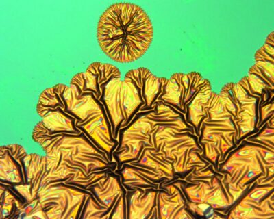
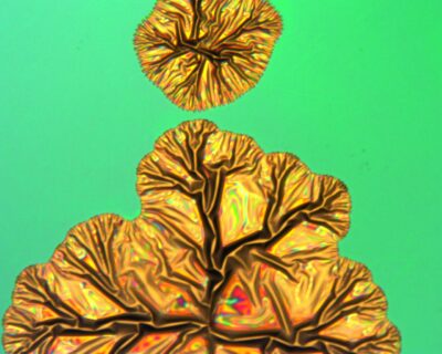
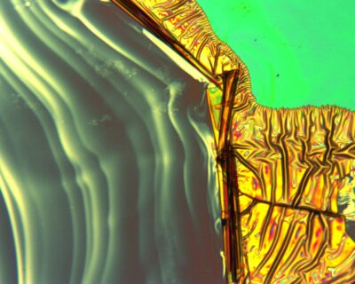
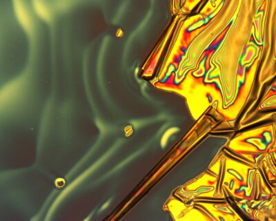
Microscopy image sequence of a representative photoresist-stripping process by aqueous, NMP-free, and sustainable fluids
The sequence shows microscopy images (100x & 200x magnification) of a representative photoresist-stripping experiment. The attacking and lift-off behaviour of different resists from various semiconductor substrates (e.g., Si-wafers) were studied in detail.
Video of a representative photoresist-stripping process by aqueous, NMP-free, and sustainable fluids
The video demonstrates a representative photoresist-stripping experiment. The lift-off behaviour of different resists were studied in detail. The formulations were optimized towards the fastest possible times to completely remove specific layers from various substrates.
Three variations of a lab-scale formation of sustainable, complex, water-based phasefluid prototype formulations for coupon level application tests:
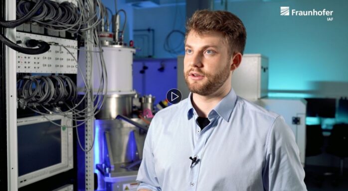
Fraunhofer IAF uses advanced cryogenic measurement capacities for quantum computing hardware in the project MATQu


This project leading to this application has received funding from the ECSEL Joint Undertaking (JU) under grant agreement No 101007322. The JU receives support from the European Union’s Horizon 2020 research and innovation programme and Germany, France, Belgium, Austria, Netherlands, Finland, Israel.